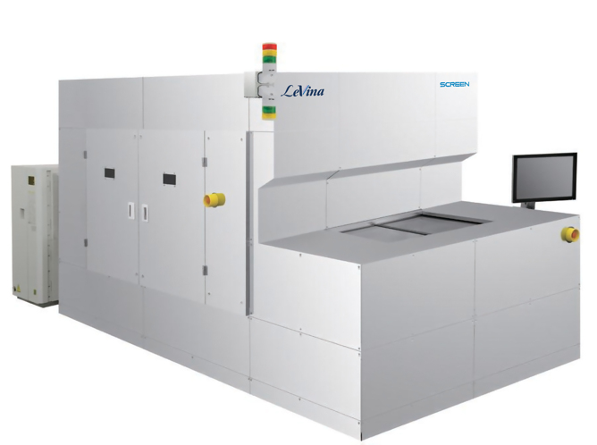
LeVina
Ucamco is proud to introduce LeVina to the European market. LeVina is the perfect Direct Imaging solution for next-gen packaging substrates.
Just like Ledia direct imagers, LeVina is Japanese technology made by SCREEN.
World-leading imaging of 2 μm
LeVina combines superior imaging heads equipped with SCREEN’s proprietary GLVTMTM optical engine and laser control technologies that utilize an optical system featuring more of SCREEN’s unique expertise. This new system is specifically designed for mass production and enables direct imaging of substrates at a market-leading resolution of 2/2 μm. It will continue to deliver high-definition patterning of advanced packages even as they become increasingly miniaturized.
Throughput of 100 substrates per hour with L/S = 5/5 μm
LeVina is fitted with an extremely reliable multi-head system and stage capable of moving at up to 480 millimeters per second. Alignment marks are read during scanning, allowing outstanding throughput regardless of the number of marks in the scanning direction (can also be automated). These features enable high resolution processing up to 100 substrates (510 x 515 mm) per hour at L/S = 5/5 μm.

Low running costs
Thanks to the laser diodes used in its light source, LeVina cuts operating costs by around 70%.
Improved cleanness
With LeVina, sources of particle generation have been blocked and it has been equipped with airflow control technologies that have a proven record in cleaning equipment for the semiconductor market. These advances have reduced contamination inside the system, helping to significantly improve yields.